
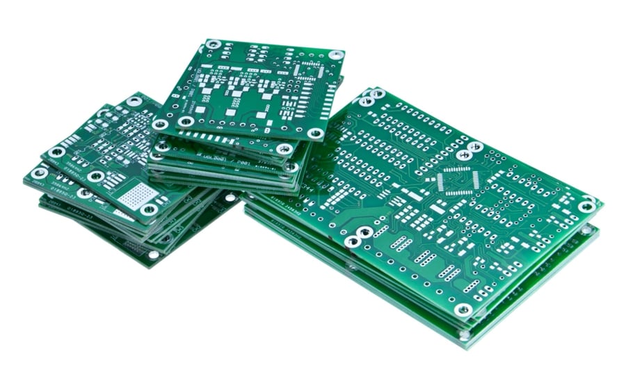
If you’ve been designing PCBs for a while, you’ve probably hit a point where your 2 layer board starts feeling cramped. Traces are getting tangled, you’re running out of room, and someone in a forum casually mentions “just go 4 layer” like it’s the most obvious thing in the world. But what does that actually mean, and is it the right move for your project?
Here’s a straightforward look at what 4 layer PCBs are, how they’re structured, and how to decide whether your build actually needs one.
The Basics: What Is a 4 Layer PCB?
A standard 2 layer PCB has exactly what it sounds like — a top copper layer, a bottom copper layer, and a fiberglass substrate (called FR4) sandwiched between them. Traces and components live on one or both of those outer surfaces.
A 4 layer PCB adds two internal copper layers buried inside the board. The typical stackup looks like this:
Layer 1 (Top) — Signal traces and components
Layer 2 (Inner 1) — Usually a solid ground plane
Layer 3 (Inner 2) — Usually a power plane
Layer 4 (Bottom) — Signal traces and components
The two inner layers are laminated between sheets of prepreg (a fibreglass/resin material) during manufacturing, creating a single rigid board that looks identical to a 2 layer board from the outside.
Why the Ground Plane Is Such a Big Deal
The single biggest advantage of moving to 4 layers isn’t the extra routing space — it’s the dedicated ground plane, and it matters more than most beginners expect.
On a 2 layer board, your ground connections are stitched together with traces, which creates resistance and inductance across the board. High-frequency signals care about this a lot. Noise creeps in, signals interfere with each other, and debugging becomes a headache.
A solid copper ground plane on Layer 2 gives every component on the top layer an extremely low-impedance return path directly underneath it. This dramatically reduces electromagnetic interference (EMI), improves signal integrity, and makes your power delivery much cleaner. For any board running at meaningful clock speeds or handling sensitive analog signals, this alone can be worth the upgrade.
The Power Plane: Clean Power Delivery
Dedicating Layer 3 to a power plane works on the same principle. Instead of routing power traces around your board — which act like little antennas at high frequencies — every component gets a direct, low-impedance connection to the supply voltage through a via.
This is particularly important for digital circuits with lots of switching activity. Every time a logic gate switches state, it draws a brief spike of current. With a power plane, that current is available almost instantly from directly below the component. Without one, the inductance of a long power trace causes tiny voltage dips — and enough of those across enough components causes unreliable behaviour that’s genuinely difficult to trace back to the root cause.
Pair the power plane with good decoupling capacitors close to your ICs and you’ve got a very solid power delivery network.
More Routing Space (And Cleaner Layouts)
The practical benefit most people think of first is simply having more room to route traces. With two full signal layers plus the ability to use the inner planes for occasional routing where needed, you can dramatically reduce board congestion.
This means shorter trace lengths, less need for vias just to get signals past each other, and cleaner separation between analog and digital sections of your board. That last point is underrated — being able to physically isolate a sensitive analog circuit from a noisy digital one on separate layers, with a ground plane between them, is a real signal integrity win.
When Does a 4 Layer Board Make Sense?
You don’t need 4 layers for everything. A simple LED controller, a basic breakout board, or a low-speed microcontroller project can live perfectly happily on 2 layers. But here are the signs it’s time to move up:
You’re working with high-speed signals. USB, Ethernet, HDMI, DDR memory, anything running at tens or hundreds of MHz — these need controlled impedance traces and good ground planes to work reliably.
You have an RF component. Wireless chips, antennas, and anything transmitting or receiving radio signals need a proper ground plane underneath them. Trying to do RF on a 2 layer board is a recipe for a noisy, low-range mess.
Your board is getting too dense to route cleanly. If you’re spending hours re-routing the same area trying to squeeze everything onto 2 layers, the time you’ll save on a 4 layer board easily justifies the extra cost.
You need clean, stable power. FPGAs, processors, high-speed ADCs, and similar components are sensitive to power rail noise. A dedicated power plane is the cleanest solution.
What Does It Cost?
4 layer boards used to be significantly more expensive than 2 layer boards, but the gap has closed considerably. At popular PCB fabs, a small 4 layer board might cost 1.5x to 2x the price of a comparable 2 layer board — not a dramatic difference for most projects.
The real cost consideration is design time. 4 layer stackups require more thought upfront: defining your layer assignment, planning your via strategy, making sure your inner planes are properly split if you have multiple voltage rails. It’s not difficult, but it’s more work than a 2 layer layout.
A Few Things to Watch Out For
Via planning matters more. Vias that connect to inner planes need to be correctly configured in your design software. Blind and buried vias are possible but add cost — for most projects, standard through-hole vias work just fine.
Plane splits for multiple voltages. If you have 3.3V and 5V rails, your power plane needs to be split into separate regions. Keep the split lines away from high-speed signal areas and make sure your ground plane remains continuous underneath them.
Check your fab’s stackup specs. Layer thickness and prepreg material affect trace impedance. If you need controlled impedance routing, use your fab’s published stackup data and impedance calculators rather than guessing.
The Bottom Line
A 4 layer PCB isn’t just about having more room to route traces — it’s about building a fundamentally better electrical foundation. The dedicated ground and power planes make a real, measurable difference to signal integrity, EMI, and power delivery that no amount of clever 2 layer routing can fully replicate.
If your project is simple and low-speed, 2 layers is fine. But once you’re dealing with fast signals, RF, dense component placement, or sensitive analog circuits, the move to 4 layers is one of the best investments you can make in the reliability of your design.
